Huawei pivots semiconductor strategy to develop 1.4nm chips amid US sanctions
Here's what it means for you.
Huawei's strategic shift towards developing 1.4nm chips by 2031 highlights the company's resilience in the face of US sanctions. This move could redefine the semiconductor landscape, emphasizing speed over traditional transistor miniaturization. As Huawei adapts its technological roadmap, stakeholders in the semiconductor industry should closely monitor these developments. The implications of this pivot extend beyond Huawei, potentially influencing global semiconductor supply chains and competitive dynamics. Companies and policymakers alike will need to consider how these advancements might reshape market strategies and regulatory approaches.
What happened
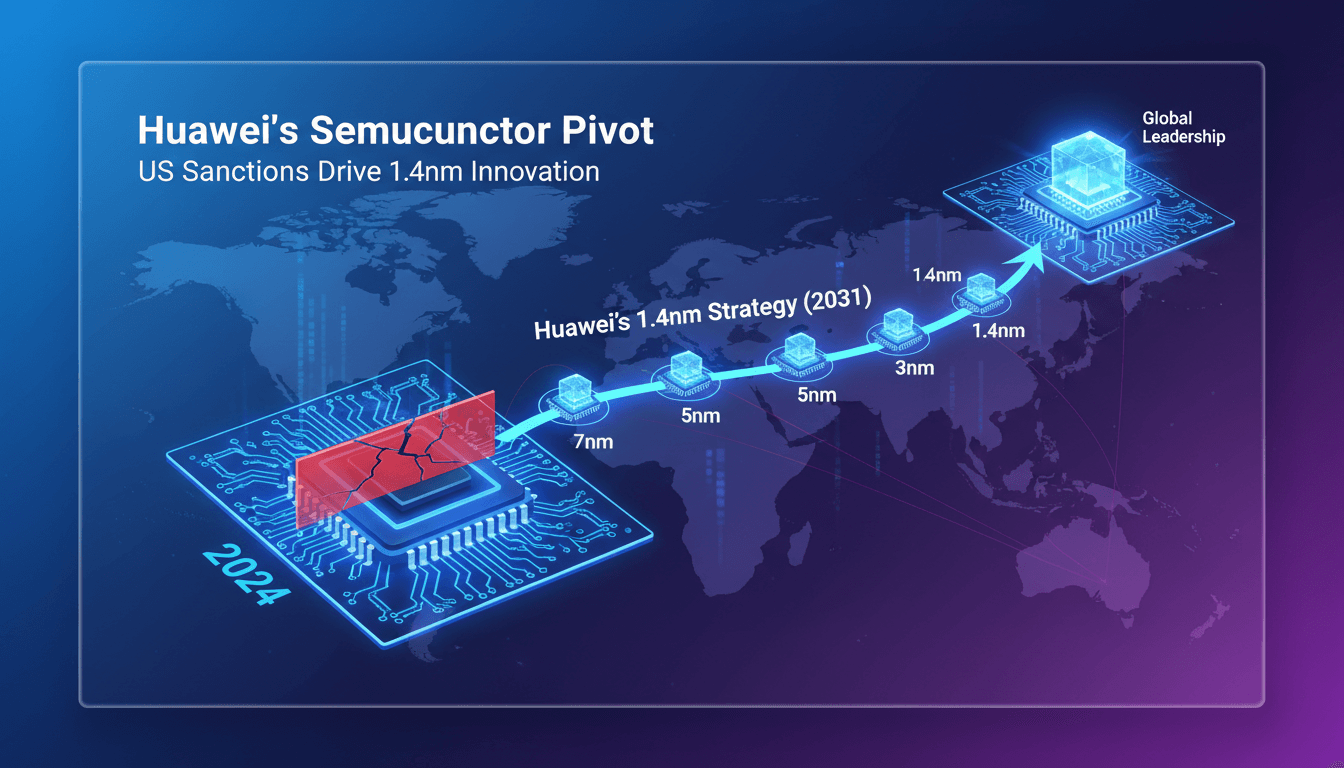
Huawei has announced a significant change in its semiconductor strategy, focusing on the development of chips with a transistor density of 1.4nm by 2031. This decision comes as a direct response to ongoing US sanctions that have restricted the company's access to advanced semiconductor manufacturing technologies. By prioritizing speed over the conventional method of shrinking transistors, Huawei aims to innovate within the constraints imposed by these geopolitical challenges.
The introduction of 'Her's Law' marks a new framework guiding Huawei's semiconductor development. This strategic pivot reflects the company's commitment to overcoming obstacles while positioning itself as a leader in semiconductor technology.
The Context
US sanctions have significantly impacted Huawei's operations, limiting its ability to access cutting-edge semiconductor technologies. In response, the company is exploring alternative methods to enhance chip performance, which could lead to breakthroughs in the industry. The shift towards a 1.4nm transistor density represents a bold move that could set new standards in semiconductor development.
As Huawei navigates these challenges, the introduction of 'Her's Law' signifies a departure from traditional approaches, emphasizing innovative solutions. This strategic evolution is crucial for Huawei's long-term viability in a competitive market increasingly influenced by geopolitical tensions.
Takeaway
Huawei's commitment to achieving 1.4nm chip density by 2031 could position it as a frontrunner in semiconductor innovation, despite the ongoing geopolitical landscape. Observers should monitor the company's progress closely, as well as any potential responses from the US government regarding these new strategies. The success of this initiative will depend on Huawei's ability to leverage technological advancements while navigating the complexities of international relations.
As the semiconductor industry evolves, Huawei's approach may inspire other companies to rethink their strategies in light of similar challenges. The outcome of this pivot could have far-reaching implications for the global technology landscape.
Regional and international reporting focused on Middle Eastern politics, diplomacy, and economics.
"Asharq Al-Awsat is a Saudi-owned international newspaper reflecting mainstream Gulf political perspectives."
— A47 Editor
Huawei Bets on Speed Over Shrinking Transistors to Sidestep US Chip Sanctions
Huawei has announced a strategic shift in its chipmaking technology, prioritizing speed enhancements over the traditional method of shrinking transistors to navigate US chip sanctions. This approach aims to maintain competitiveness in the semiconduct...
Market-moving headlines impacting equities, bonds, and related risk assets.
"Real-time catalysts and volatility drivers across indices and sectors."
— A47 Editor
Analysis-Huawei bets on speed over shrinking transistors to sidestep US chip sanctions
Huawei is focusing on speed rather than shrinking transistors to navigate the challenges posed by US chip sanctions, as detailed in a recent analysis. The company aims to enhance its semiconductor capabilities through innovative strategies, including...
Policy and strategy for digital leaders, including AI.
"Analyzes AI in the context of enterprise strategy."
— A47 Editor
Huawei unveils plan for 1.4nm chip density as US sanctions persist
Huawei Technologies has announced plans to develop semiconductors with a transistor density equivalent to 1.4-nanometre (nm) processes by 2031, despite ongoing US sanctions. This strategic move highlights the company's commitment to advancing its tec...
Electronics industry news including AI chips.
"Covers semiconductors and embedded AI trends."
— A47 Editor
Necessity is the Mother of Invention: Huawei Replaces Moore’s Law With Her’s Law
Huawei has introduced a new chip design approach called the 'Tau Scaling Law' at the IEEE International Symposium on Circuits and Systems in Shanghai, marking a significant shift from traditional transistor miniaturization to reducing signal-propagat...